Bipolar Junction Transistor (BJT)
- BJT is a three-layer semiconductor device consisting of two PN junctions.
- N-type material is sandwiched between two layers of P-type, the transistor is known as the PNP transistor.
- On the other hand, a layer of P-type material is sandwiched between two layers of N-Type, the transistor is known as NPN transistor.
- The center layer is the base, the left layer is the emitter and the right layer is a collector.
- EMITTER = E,
- BASE=B,
- COLLECTOR=C,
- The emitter layer is heavily doped it emits electrons if the transistor is of NPN type (emits holes if the transistor is of PNP type) to the base.
- The base is lightly doped and the doping level of the collector is intermediate.
- The collector is so named because it collects electrons if the transistor is of NPN type (collects holes if the transistor is of PNP type) from the base.
- The collector is the largest of the three regions.
- To have a better understanding of transistors we will concentrate on NPN transistors in the next sections.
 |
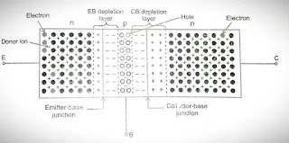
| Bipolar junction transistor construction |
- Let us consider the NPN transistor shown in Fig.
- There are two junctions in it.
- One is between emitter and base and the other is between collector and base.
- Because of their repulsion, the free electrons on then sides diffuse across the emitter-base junction and recombine with the holes in the base.
- Similarly, the electrons in the collector diffuse across the collector-base junction.
- When a free electron in the n-layer diffuses across the junction, it leaves the parent pentavalent atom in the n-layer and makes it a positive ion.
- After diffusion, it combines with the parent trivalent atom in the p-region making it negative.
- As a result, a layer of depleted carriers is formed at the junction.
- This layer of depletion without free charge carriers is known as the depletion layer.
- Beyond a certain point, the depletion layer acts as a barrier to further diffusion of free electrons across the Junction.
- The difference of potential across the diffusion layer is called barrier potential.
- Since the doping levels of the three layers are different, the thickness of depletion layers does not have the same width.
- As the emitter is heavily doped, the concentration of ions near the junction is greater; hence the depletion layer penetrates slightly into the emitter region.
- But the depletion region penetrates deeply into the base, as it is lightly doped.
- As the collector layer is moderately doped, the depletion layer width in the collector is more than the depletion layer width in the emitter.
- Hence the depletion layer width in the emitter-base junction is less than the depletion layer width in the collector-base junction.
 |
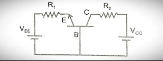
| Bipolar junction transistor block diagram |
Transistor Biasing
 |
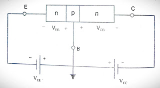
| Transistor with EB, CB junctions reverse biased |
 |
| Transistor with EB, CB junctions reverse biased |
 |
| Transistor with EB and CB junctions forward biased |
- For the proper operation of a transistor, the two PN junctions must be correctly biased with external de voltages. Fig shows an NPN transistor in which the emitter-base and collector-base junction are forward biased.
- Since both junctions are forward biased the emitter and collector currents are large. Fig shows the transistor in which both emitter-base and collector-base junctions are reverse biased.
- In this case, the currents are due to thermally generated minority carriers.
- The third type of bias is most commonly used to operate the transistor as an amplifier. In this bias, the emitter-base junction is forward biased and the collector-base junction is reverse biased.
Operation of NPN Transistor
 |
| Transistor with forward-biased EB junction and reverse biased CB junction |
 |
| Transistor with reverse biased EB junction and reverse biased CB junction |
 |
| Transistor with forward-biased EB junction and reverse biased CB junction |
- Now we discuss the basics of the operation of an NPN transistor. Fig Shows an NPN with a forward-biased emitter-base (EB) junction and a forward-biased collector-base(CB) junction.
- Due to forward bias, the barrier potential at the EB junction and at CB Junction reduces and electrons flow from n-type to p-type.
- Both the emitter and collector currents are large.
- When both junctions are reverse biased the flow of current is due to thermally generated minority carriers.
- This thermally produced current is temperature-dependent.
- It approximately doubles for every 10°C rises in ambient temperature.
- For a normal transistor operation, the EB junction is forward biased and the CB junction is reverse biased.
- When EB junction is forward biased the barrier potential reduces and causes a large number of electrons to flow from the n-type emitter to the p-type base.
- Since the base is very thin and lightly doped a small portion (1% to 4%)of base electrons will recombine with holes and constitute a base current.
- The magnitude of base current is typically in the order of microamperes.
- The electrons that are not recombined in the base region are collected by the collector and constitute a collector current.
Operation of a PNP Transistor
- The operation of a PNP transistor can be explained using Fig. In Fig the emitter-base junction and collector-base junctions are forward biased.
- Hence both the emitter and collector currents are large.
- Fig shows the PNP transistor when both the junctions are reverse biased.
- In this case, the emitter and collector currents are small and are due to thermally generated minority carriers.
- In Fig the emitter-base junction is forward biased and collector-base junction is reverse biased.
- The forward biased emitter-base junction causes a lot of holes to cross from the emitter region to the collector region.
- Since the base is lightly doped the number of electrons in this region is small.
- Hence the number of holes combining with electrons in the base is also small which results in a small base current.
- The remaining holes that are not combined (more than 95%) cross collector-base junction to constitute a collector current.


Post a Comment