
PN Junction Diode
- Fig shows a PN junction diode formed by the two blocks of semiconductor material; one of p-type material and the other of n-type material.
- In the p-region, the holes are majority carriers and electrons are minority carriers, whereas in the n-region electrons are majority carriers and holes are minority carriers.
- The holes in the p-region are represented by small circles and the electrons in the n-region are represented by dots as shown in Fig.

- Since the concentration of electrons in an n-region is more compared to the p-side, free electrons from the n-side diffuse across the junction and fill the holes on the p-side. (Diffusion is a natural process through which charges flow from higher to lower concentration until the difference in concentration is eliminated).
- Similarly, the holes from p-side diffuse across the junction and recombine with electrons in the n-side.
- The free electrons that cross the junction create positive ions (since an atom lost one electron) on the n-side.
- Similarly, the diffusion of holes in the p-material creates negative ions. Since negative ions are created on the p-side of the junction, the region close to the junction acquires a negative charge.
- Similarly, thè positive ions created on the n-side give a positive charge near the junction. The charge density p on the two sides of the PN junction is shown in Fig.
- The shape of the charge density p depends on the doping level of the diode.
- As these charges build up a point is reached where the total negative charge in the p-region repels any further diffusion of electrons (negatively charged particles) into the p-region (like charges repel) and the diffusion stops.
- At this point, the positive ions on the n-side and negative ions on the p-side are immobile (fixed). They cannot serve as current carriers.
- The carriers originally present (before diffusion) in this region, have traversed the junction to combine with the atoms on the other side.
- As a result, the junction region is almost completely depleted of carriers. This region near the junction is called the depletion region, space charge region, or transition region.
- The width of the depletion region is about 1um(10 m). Since there are many positive charges and many negative charges on opposite sides of the PN-junction an electric field is formed.
- The electric field produced is a barrier to the flow of free electrons in the n-region, and energy must be spent to move an electron through the electric field.
- That is external energy must be applied to move an electron through the electric field. The external energy depends on the potential difference of the electric field across the depletion region. This potential difference that is required to move electrons through the electric field is known as barrier potential (Vo) and it is expressed in volts.
- The magnitude of V is of the order of a few tenths of volts. This value is 0.3V for a Ge and 0.7V for Si.

- The depletion layers on each side of the junction are equal in thickness if the doping densities of the p-side and n-side are equal.
- On the other hand, if the p-side is more heavily doped than the n-side, then depletion layer thickness in the n-side is more than that of the p-side.
- This is to encompass an equal number of impurity atoms on each side of the junction. Similarly, if the n-side is heavily doped, then the depletion layer thickness in the p-side is more than that of the n-side.


Bias


- When an external source is connected to a device, then that device is said to be biased. When the positive terminal of a battery is connected to the p-side of the device and the negative terminal is connected to the n-side of the device, then the device is said to be forward-biased.
- On the other hand, if the negative terminal is connected to the p-side and the positive terminal is connected to the n-side, then the device is said to be reverse biased.
The forward biased PN junction
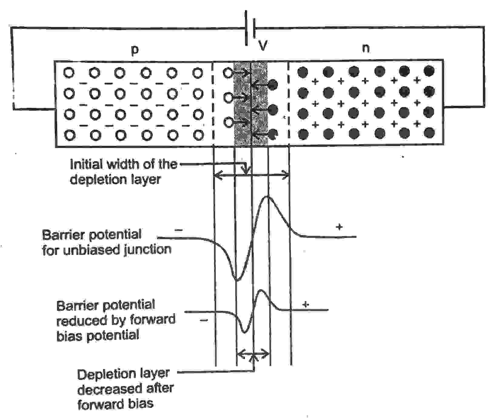
- When an external potential V volt is applied across the PN junction such that the positive terminal is connected to the p-type material and the negative terminal is connected to the n-type material, then the diode is said to be forward-biased. A forward-biased PN-junction is shown in Fig(a).
- When a forward bias is applied to the PN-junction the holes in the p-side are repelled by the positive terminal of the battery and flow towards the junction.
- Similarly, the electrons in the n-side are repelled by the negative terminals of the battery and move towards the junction. These electrons and holes that are driven towards the junction recombine with the ions near the boundary and reduce the width of the depletion region as shown in Fig. This reduction in the width of the depletion layer reduces the barrier potential.
- If the applied voltage is increased further, a stage is reached where the barrier potential effectively disappears and charge carriers can easily flow across the junction.
Reverse bias

- If an external potential V volts is applied across the PN-junction such that the positive terminal of the battery is connected to n-side material and the negative terminal is connected to p-side material, then the diode is said to be reverse biased.
- Fig shows a reverse-biased PN junction diode. The reverse bias forces the free electrons in the n-region to move away from the junction towards the positive terminal. These electrons leave more positive ions near the junction.
- Similarly, the holes in the p-side also, move away from the junction towards the negative terminal of the battery. These holes leave more negative ions near the junction. As a result, the width of the depletion region increases.
- The greater the reverse bias, the wider the depletion layer. This increase in the width of the depletion region effectively reduces the majority carrier flow.
- However, due to thermal energy-limited number of free electrons and holes are generated in p-side and n-side of the PN-junction respectively. Electrons in the p-side move towards the right and cross the junction and holes in the n-side move towards the left and cross the junction.
- The movement of minority carriers constitutes a current known as reverse saturation current denoted as Ico. Since Ico is due to thermally generated minority carriers it will not increase with the increase in reverse voltage.
- It increases with an increase in temperature. Normally it doubles for every 10°C rises in temperature. The reverse saturation current Ieo is typically less than IpA for silicon, while for germanium it may exceed 10uA.
Breakdown voltage
If the reverse-biased voltage is increased, the velocity of minority charge carriers crossing the junction increases. The greater the reverse bias the faster the electron moves. Since velocity increases, the associated kinetic energy (mu) also increases.
When these carriers with high kinetic energy collide with an atom, the valence electron in the atom absorbs sufficient energy and leaves the parent atom. These additional carriers also get sufficient energy from the applied reverse bias and collide with other atoms and generate some more carriers. This collision and generation of carriers is a cumulative effect, which results in a large amount of reverse current. This phenomenon, known as reverse breakdown occurs at a particular reverse voltage for a PN-junction.
This voltage is known as the reverse breakdown voltage.
Diode Characteristics

The circuit diagram to obtain the volt-ampere characteristics of a diode is shown in Fig. It consists of a dc voltage source and a resistor connected in series with a diode. A resistor is used to limit the forward current to a value that will not overheat the diode and cause damage. An ammeter is connected in series with the diode to measure the diode current ID and a voltmeter is connected across the diode to measure the voltage across it. By varying the dc voltage source the voltage Vp across the diode and current Ip through the diode can be measured.
When the applied voltage is zero, the voltage across the diode remains zero; hence there is no forward current. When the applied voltage is increased gradually, the forward current and the voltage across the diode gradually increase. When the applied voltage increases to a value that increases the voltage across the diode to barrier potential (0.7V for Si, 0.3V for Ge), the forward current begins to increase rapidly. The V-I characteristics of a forward-biased diode are shown in Fig. The diode forward voltage(Vr) and the diode forward current(Ip )are taken on X-axis and Y-axis respectively. From Fig. we can see that the forward current is very low until the voltage across a junction reaches approximately 0.7V. After this point, the current Ip increases rapidly. But the forward voltage remains at 0.7V. This point on the l curve where the forward voltage approximately equals the barrier potential is known as the knee of
the characteristic curve. The corresponding voltage is also known as knee voltage or cut-in voltage of the diode.
V-I characteristic of a reverse-biased diode

To find the V-I characteristic of a diode in reverse bias, we simply reverse the position of the diode as shown in Fig. As the reverse bias increases from zero, a small reverse saturation current flows through the diode and the voltage across the diode increases. When the applied reverse bias reaches a certain value, a reverse avalanche breakdown would occur; then the magnitude of the current increases rapidly as shown in Fig. This voltage at which the diode current increases rapidly is known as the reverse breakdown voltage.
Avalanche breakdown
When a PN junction diode is reverse biased, the thermally generated minority carriers constitute the flow of reverse saturation current through the diode. These carriers acquire energy from the applied potential and collide with crystal ions. As a result, the covalent bonds are disrupted and new electron-hole pairs are generated. The additional pairs generated in this way also pick up sufficient energy from the applied potential and generate additional electron-hole pairs by collision. Thus each new charge carrier, in turn, produces an additional charge carrier by breaking the covalent bonds. As a result, the number of charge carriers avalanche increases to peak level and results in avalanche breakdown.
Zener breakdown
When the p and n regions are heavily doped, the width of the depletion region becomes very small. As a result, a small voltage (around 5V) can produce high electric field intensity within the narrow depletion region. Under the influence of high electric field intensity direct rupture of covalent bonds takes place. The new electron-hole pairs thus created increase the reverse saturation current.
It is found that Zener breaks down occurs at a field of approximately 2x 10 VM.
For heavily doped diodes this value is reached at about 5V. Hence for heavily doped diodes, Zener breakdown is the predominant effect. For lightly doped diodes the breakdown voltage is higher; hence avalanche multiplication is the predominant effect.
Temperature characteristics
Zener breakdown occurs in heavily doped diodes due to the fact that in these diodes, the depletion width is narrow and hence high electric field intensity. When the temperature is increased the valence electrons acquire energy and escape from the covalent bonds. Hence less applied voltage is required to convert valence electrons to conduction electrons. As a result, Zener's breakdown voltage decreases with temperature.
A lightly doped diode with a broad depletion layer will break down by the avalanche multiplication. Note that avalanche multiplication depends on collisions of carriers with crystal ions. When the temperature has increased the vibration of atoms in the crystal increases which increases the probability of collisions. As a result, the intrinsic holes and electrons have less opportunity to start the avalanche process. Therefore the avalanche voltage increases with increasing temperature.
pn Diode Applications
The PN junction diode allows the flow of current in one direction and blocks current in the other direction. This property of diode can be used in various applications, Some of the applications are listed below
1. Rectifiers in dc power supplies.
2. Clippers in wave shaping circuits.
3. Clampers in TV receivers.
4. Voltage doublers in CRT.
5. Switching in digital logic circuits.
6. Diode gates.
7. Comparators.
thank you SIR
ReplyDeletePost a Comment